
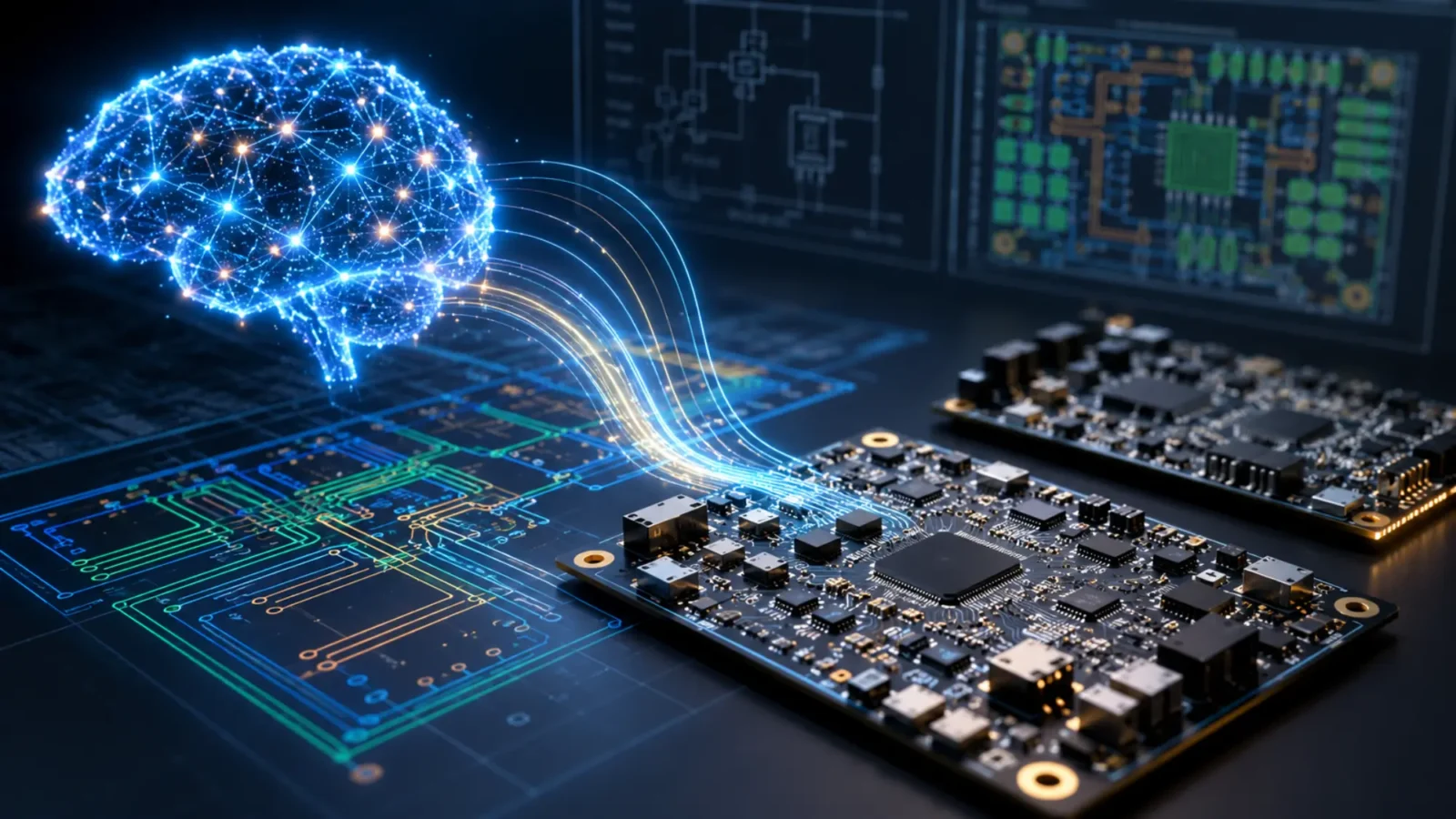
OpenAI’s GPT-6 Astra converted an electronic schematic into a manufacturable printed circuit board in KiCad in less than 3 minutes.
The demonstration is impressive by its speed. What Astra did, is the more important thing.
Astra worked directly inside the engineering software, placing components and routing the PCB on its own, instead of taking an engineer through a full tutorial on PCB design. It did all the copper connection placement and routing itself.
This puts AI one step closer to being able to do engineering, rather than just give engineering advice.
Electronics engineers have used AI tools for years to read datasheets, explain circuits, suggest component values, troubleshoot problems and generate firmware. Automating the design of physical circuit boards has proved to be much harder, as each decision made on the screen can have a huge impact on how the board will actually work.
A copper trace is more than just a line between two points. It sends a signal or power.
Moving a component changes the trace lengths. Return paths are subject to change. Heat can move through the board differently. Noise levels could increase. You may encounter electromagnetic interference and signal integrity issues.
High speed digital designs may need controlled impedance and carefully matched trace lengths. In power circuits two factors must be taken into account: the current density and the heat. You may need to isolate sensitive analogue sections from noisy switching circuits.
So a PCB can look perfect in KiCad and still not work when it is finished building.
That distinction is what matters when considering Astra’s demonstration.
Astra demonstrated that a frontier AI model can run PCB software, place components and route a board. That does not imply that all the electrical or physical decisions made by the board are correct.## Verification is maybe more important than generation
EEBench has a different approach to AI electronics.
EEBench employs deterministic engineering tests to validate the electrical requirements of a design, not to investigate if an artificial intelligence can generate a circuit that appears plausible.
This is illustrated by the following task.
The processor of a household energy meter shall continue running for an additional 20 ms after loss of its 5 V input. The protected power rail should remain above the 3.0 V brownout threshold during this time.
Adding a capacitor sounds like an easy fix.
In the case of real components it is somewhat less simple.
A capacitor marked 22 uF in the real world may not be 22 uF in operation. The effective capacitance of ceramic capacitors can be significantly reduced by DC bias. Voltage rating, package size, tolerance, cost and recharge behaviour are also important;
A documented EEBench design, nominal 22 uF capacitor was found to be 11.4 uF at 4.7 V bias. EEBench found 545 µF was required for the task. In simulation, the protected rail fell below 3 V after only 0.85 milliseconds, whereas it remained above the threshold for the required 20 milliseconds.
The scheme of the circuit seemed plausible.
Physics threw it out.
The biggest challenge for AI-generated hardware may be the difference between a physically valid design and a plausible answer.# Hardware needs a feedback loop
Software agents have one big plus: testing fast.
An AI coding agent can generate code, compile it, run tests, diagnose an error, modify the code and start another try in seconds.
Hardware development generally takes a good bit longer.
Mistakes can slip through schematic review, PCB layout and fabrication, only to be found by engineers during board bring-up. At this point it may be necessary to do an additional manufacturing cycle and revise the board.
Simulation can accelerate part of that process.
An AI system could modify a circuit and then run a SPICE simulation, measuring voltage, ripple, gain, thresholds, transient behaviour and other requirements. Any components that failed could be revised.
This allows for a much better engineering loop:
Generate → Emulate → Measure → Correct → Validate
Time saving measure . Producing ten PCB layouts quickly.
Changing the way electronic products are developed could involve automatically generating those layouts, testing them, identifying failures, correcting the designs and subsequently testing them.
Fast routing is a good thing. Fast iteration has a big advantage.# It may be that AI does not need PCB software that is designed for humans.
Further modifications are possible in the future under the graphical interface.
In PCB software you have schematic pages, symbols, footprints, menus, layers, board views, etc. All of these are for human understanding and modification of the designs.
AI doesn’t have to work this way.
EEBench employs atopile, a declarative system that describes electronic designs as structured code. An AI agent can deal directly with components, electrical connections, constraints, instead of using some of its context to track windows, menus, cursor positions and other interface details.
Product requirements could be specified as structured constraints to initiate machine orientated design processes.
The AI could, for example, first suggest an architecture, select components, generate an electrical design, simulate its behaviour, correct failures, and only then move on to component placement and PCB routing.
The process could be advanced by EDA software incorporating design-rule checks, signal integrity analysis, power integrity analysis, thermal testing and manufacturability checks.
And the human engineers would still decide if the result is good enough to be built.
A PCB layout is only one part of a much larger machine-readable engineering model that links requirements, components, simulations, constraints and physical design within that workflow.# Cadence, Siemens embedding AI deeper in EDA
OpenAI’s not the only one working on this.
Cadence launched the AuraStack AI Super Agent for PCB and advanced packaging workflows in July 2026. AuraStack is designed to bring AI to areas such as system planning, physical implementation, design constraints, manufacturability and multiphysics analysis when used with Allegro AI Studio.
Better than regular autorouting.
In real products there is an interaction of electrical, mechanical, thermal and manufacturing decisions. Connecting those regions transforms PCB automation into a larger engineering orchestration challenge.
Siemens announced agentic AI workflows that self-verify for semiconductor and PCB design in July 2026.
It combines AI orchestration with deterministic physics based EDA tools. The language models can read the requirements, use complex software, and look for alternatives. The engineering solvers can check the choices against measurable physical requirements.
That division of labour makes sense.
Language models say.
Physics has to be validated.# Flux and CELUS start with product intent.
Other organisations are tackling the problem earlier in the design process.
Engineers can tell Flux what design they want to build and Flux will help them with component research, planning, bills of materials, schematic work, placement, routing and preparing to manufacture.
It can also expose real PCB context such as pins and nets to external AI agents using MCP.
This can be especially useful when hardware and software development overlap. A coding agent that understands the real structure of the circuit has a much more valuable context when generating firmware for the hardware.
And CELUS starts with the product specifications.
The platform links those requirements to reference designs and components to generate engineering outputs such as schematics and bills of materials for integration into existing EDA environments.
Translation is a key part of electronics engineering. Product requirements are translated into functions, functions are translated into component choices, schematics and physical hardware.
AI does not have to take the place of an electrical engineer just to speed things up.
Reducing the amount of manual translation is already valuable.# Quilter demonstrates the impact of building boards designed by AI.
Simulation is good, but pretending you have hardware is better.
Quilter’s Project Speedrun shows that an AI-assisted PCB layout can result in a working physical product.
The Linux computer was created by Project Speedrun based on the NXP i.MX 8M Mini with two 8-layer PCBs. Published project figures claim 843 components and 5,141 pins.
It was estimated that manual PCB layout would take 428 hours.
Overall, the human effort put in on Quilter was around 38.5 hours.
When ready, the computer had booted successfully, said Quilter.
| Measurement | Project Speedrun |
|---|---|
| Boards | 2 |
| PCB layers | 8 |
| Components | 843 |
| Pins | 5,141 |
| Quoted manual PCB layout | 428 hours |
| Human work with Quilter | About 38.5 hours |
Note that human cleanup was still necessary.
In Project Speedrun, AI isn’t seen designing every component of a complex computer separately. It shows a more practical side of the present state of the art: engineers can compress a lot of layout work but still be involved in reviewing and correcting what gets produced.
The question of where humans came into the picture of the development of PCBs is moot.
It is the extent to which engineering jobs can be automated without sacrificing the necessary oversight to catch costly mistakes. OpenAI’s GPT-6 Astra and EEBench measure different capabilities
Comparing Astra to EEBench would be misleading.
Astra’s KiCad demo is a test of an AI model’s ability to run PCB design software and produce a physical layout.
EEBench then runs simulations of the AI-generated circuits and evaluates them against the target electrical specifications.
The benchmark report dated September 4, 2026, as referenced in the source material, did not include Astra’s EEBench score.
In addition, EEBench V1 does not evaluate whether an artificial intelligence can design, manufacture, assemble and bring up a complete electronic product by itself.
They therefore answer different questions.
These layers will need to be connected in future hardware benchmarks: requirements, circuit correctness, realistic component behaviour, schematic design, PCB layout, physical constraints, manufacturability, and ultimately, functional hardware.
Building a board on a screen is only half of the test.# Engineering judgement is still hard to automate.
There is no one perfect solution to the problem of PCB design.
The smaller the board the smaller the product . The smaller the board the more difficult to cool .
Increasing the board area but maintaining a larger spacing can improve the electrical behaviour.
Lower cost components may reduce the bill of materials, but may also introduce reliability or availability problems.
Adding more simulation will reduce the chance of a costly board respin, but it will also extend the development schedule.
If the component is technically superb, but has a lead time of 40 weeks, it might not be a good choice.
The artificial intelligence can sift through far more potential designs than a human engineer could realistically examine by hand.
There is still a requirement for an individual to decide which aspects should be optimised.
Cost, size, reliability, performance, manufacturing risk, supply availability, thermal behaviour, development time and many other priorities often compete with each other.
Those priorities are based on engineering and business judgement, not just PCB routing.The biggest change is the closed loop engineering.
PCB autorouters have been around for decades so to reduce this change to “AI is able to route circuit boards” is an oversimplification of the extent of change that is going on.
Modern systems are linking up stages that were run separately:
Requirements → Component selection → Schematic → Simulation → Placement → Routing → Physical analysis → Manufacturing checks → Revision
Revision is perhaps the most important part.
Once an AI system can observe the results of deterministic engineering tests , and adapt its own design accordingly , hardware development begins to get a rapid feedback loop , which software agents already use effectively .
The first printed circuit board (PCB) made by an artificial intelligence (AI) might not be very important.
If every iteration has been tested and improved automatically, the fifth or the tenth or the twentieth version might be of great importance .
That changes the economics of doing hardware development.
Startups have the ability to reject bad designs before they pay for fabrication. Robotics teams can speed up electronics revisions when firmware or mechanical requirements change. Automotive teams may want to explore additional combinations of electronics, thermals and packaging before freezing a product.
The value is not only in the expedited routing of a single board.
This is because other ideas are investigated before the point where the physical decision-making process becomes too costly to undo.
Artificial intelligence can now do large parts of a PCB and circuit design. You can see the progress in Astra’s KiCad demo, which was 2 minutes and 54 seconds long.
But the copper trace drawing is not the end of the job.
Engineers will be able to design, test the design against physical requirements, find the problem, fix it and repeat till they are confident enough in the result. This will be for more substantial systems.
And at that point, the question of can AI design a circuit board might be the wrong question.
The more pertinent question is how many designs an engineering team can research, discard, validate, and improve before sending one to fabrication.